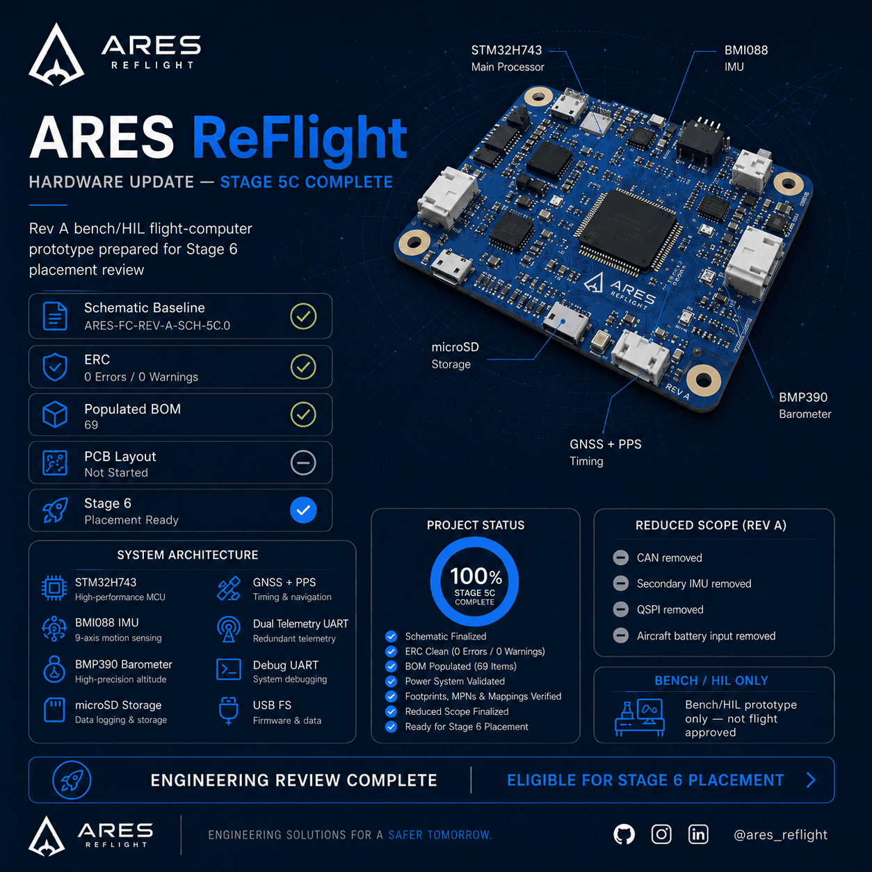
ARES-FC-REV-A-SCH-5C.0 is a BENCH/HIL PROTOTYPE and is NOT FLIGHT APPROVED. Stage 5C schematic closure does not mean that PCB placement, routing, fabrication, assembly, bring-up, environmental testing, or flight validation has been completed.
Why Rev A was reduced
Rev A was deliberately narrowed to reduce simultaneous unknowns before physical layout. The objective is not to place every future interface on the first board. It is to create a traceable flight-computer baseline whose power, sensing, storage, programming, and communications paths can be reviewed and measured on the bench.
Removing lower-priority functions reduces routing density, power-domain complexity, connector count, firmware surface area, and the number of failure modes that would otherwise have to be diagnosed during first bring-up. This is a prototype risk-control decision, not a statement that the removed functions have no future value.
Rev A is intentionally a focused bench/HIL learning platform. Reduced scope is being used to improve inspectability before physical PCB design begins.
Final retained architecture
The retained architecture centers on the STM32H743ZIT6 and keeps only the interfaces required to evaluate a practical first flight-computer prototype. The BMI088 remains the primary inertial sensor, the BMP390 provides barometric sensing, and the Molex 104031-0811 socket provides removable microSD logging.
- STM32H743ZIT6 microcontroller.
- BMI088 primary IMU.
- BMP390 barometer.
- Molex 104031-0811 microSD socket.
- GNSS UART with PPS timing input.
- Telemetry A and Telemetry B.
- Debug UART.
- USB 2.0 Full-Speed device interface.
- Tag-Connect SWD programming and debug.
- Dedicated reset and BOOT0 access.
- Status LEDs and engineering test points.
What Stage 5C closed
Stage 5C establishes the named schematic baseline ARES-FC-REV-A-SCH-5C.0. The closure review covered population state, electrical-rule checks, footprint assignment, manufacturer-part-number binding, and symbol-to-pad mapping.
These checks make the design eligible for Stage 6 PCB placement consideration. They do not prove that the selected parts are available, mechanically suitable, correctly oriented in a physical assembly, thermally adequate, or electrically correct under real operating conditions.
| Closure check | Verified result |
|---|---|
| Populated BOM | 69 components |
| DNP | 0 |
| ERC errors | 0 |
| ERC warnings | 0 |
| ERC exclusions | 0 |
| Missing footprint assignments | 0 |
| Missing exact MPNs | 0 |
| Symbol-to-pad mismatches | 0 |
Clean automated checks are necessary evidence of schematic closure. They are not evidence of a completed or manufacturable PCB.
Power architecture decision
The 3.3 V rail is bound to the TPS62162DSGR, a 1 A buck regulator. The input protection baseline uses the Littelfuse 0467.001NRHF 1 A fuse. This creates a concrete power implementation for placement review instead of leaving the regulator and protection strategy as generic symbols.
The Rev A board does not accept aircraft-battery input directly. Its input-power boundary must remain compatible with the intended bench/HIL supply and later system-level power architecture. Stage 6 will examine current-loop area, regulator component placement, return paths, thermal separation, and access for measurement.
The 1 A regulator and fuse selections are schematic bindings. Load transients, thermal rise, conversion margin, and protection behavior still require physical measurement.
Sensor and logging architecture
The BMI088 is retained as the sole Rev A IMU so that mechanical placement, vibration coupling, power integrity, and interface behavior can be evaluated without introducing a second inertial sensor and its associated comparison logic. The BMP390 uses a 400 kHz I2C interface at address 0x76 with 4.7 kΩ pull-ups on SDA and SCL.
The microSD interface uses SDMMC1 in four-bit mode. CMD and DAT0–DAT3 each use 47 kΩ pull-ups, while card detect uses a 10 kΩ pull-up. The Molex 104031-0811 footprint is the exact retained socket binding.
First power-up measurements will include BMP390 bus rise time and microSD peak current. Those measurements will be compared with the actual assembled board and firmware access pattern; the schematic values alone do not establish signal-integrity or current-margin acceptance.
USB and communications interfaces
USB is retained as a USB 2.0 Full-Speed device interface. VBUS presence is sensed on PA9 as a GPIO through a 39 kΩ / 82 kΩ divider, with VBDEN disabled. First power-up will measure the resulting PA9 voltage instead of assuming that the calculated divider behavior is sufficient.
External communications are intentionally separated into GNSS UART plus PPS, Telemetry A, Telemetry B, and a Debug UART. This preserves distinct paths for navigation timing, operational telemetry experiments, and bring-up diagnostics without adding the removed CAN or external expansion interfaces.
- GNSS data uses UART; PPS remains a separate timing signal.
- Telemetry A and Telemetry B remain independent schematic interfaces.
- Debug UART remains available for controlled bring-up.
- USB device operation and VBUS sensing require bench validation.
Exact connector strategy
Connector intent is now explicit at the schematic boundary: Molex 104031-0811 for removable microSD, Tag-Connect for SWD, a dedicated USB device connection, and separate access for GNSS/PPS, Telemetry A, Telemetry B, Debug UART, reset, BOOT0, status LEDs, and test points.
Stage 5C does not close the mechanical connector review. Physical samples, mating-part checks, pin-one orientation, cable exit direction, retention, assembly access, and a 1:1 printed footprint sign-off remain required before placement can be accepted.
An exact library footprint is not a substitute for checking a physical component and its mating system against a 1:1 board print.
What was deliberately removed
The following functions were removed from Rev A to keep the first physical design review bounded. Their removal must remain visible so later readers do not infer capabilities that are absent from the baseline.
- CAN.
- Secondary IMU.
- QSPI.
- External ADC connector.
- External status/safety connector.
- Buzzer.
- External HSE and LSE.
- Aircraft-battery input.
Removed from Rev A does not mean rejected permanently. Reintroduction requires a later requirement, architecture review, and a new controlled baseline.
What Stage 6 placement will examine
Stage 6 begins physical PCB design with placement review, not routing. The first task is to establish mechanical and functional constraints before copper paths make those decisions expensive to change.
- Board outline and usable keep-out regions.
- Mounting-hole location, fastener clearance, and structural load paths.
- Connector access, cable exit direction, insertion clearance, and serviceability.
- BMI088 mechanical isolation, orientation, and distance from vibration and heat sources.
- BMP390 pressure-port protection, airflow exposure, contamination risk, and enclosure interaction.
- Buck-converter thermal and electromagnetic separation from the IMU and barometer.
- USB and microSD edge placement for physical access and controlled routing.
- Preliminary 3D mechanical review before routing begins.
Historical Stage 5C boundary: placement and routing had not started when this schematic-closure record was written. Stage 6 placement is now complete; routing remains unstarted.
Remaining human verification
Automated closure results cannot confirm every library, sourcing, assembly, or mechanical assumption. Before placement approval, each critical footprint must be checked against the current manufacturer drawing and, where practical, a physical sample.
The review must include pin numbering, exposed-pad mapping, polarity, package variant, assembly orientation, connector mating, component height, courtyard clearance, test-point access, and availability of the exact manufacturer part number. A 1:1 printout and preliminary 3D assembly review remain mandatory human gates.
After assembly, first power-up measurements will include USB PA9 voltage, BMP390 rise time, microSD peak current, and buck-converter temperature. Additional rail, reset, clock, programming, interface, and sensor checks will be defined in the bring-up procedure before power is applied.
What this milestone does not prove
Stage 5C does not prove flight readiness, certified-avionics compliance, PCB manufacturability, signal integrity, power integrity, thermal margin, sensor performance, vibration tolerance, electromagnetic compatibility, environmental durability, firmware correctness, or safe aircraft integration.
No Gerbers, manufacturing package, or fabrication order exists. No PCB routing has started. No board has been manufactured, assembled, powered, tested in HIL hardware, installed in an aircraft, field tested, or flight validated.
The correct claim is narrow: the Rev A schematic baseline is closed against the listed checks and is eligible to enter placement consideration under continued human review.
ARES-FC-REV-A-SCH-5C.0 remains a BENCH/HIL PROTOTYPE and is NOT FLIGHT APPROVED.
Challenge the assumptions.
We welcome technical review, sourcing suggestions and manufacturability feedback before placement and routing begin.