DIGITAL PLACEMENT EVIDENCE ONLY. ARES Flight Computer Rev A remains a BENCH/HIL PROTOTYPE and is NOT FLIGHT APPROVED. Stage 6 does not prove physical fit, manufacturability, assembly, power-up behavior, thermal performance, sensor performance, environmental tolerance, or flight readiness. No routing, Gerbers, manufacturing package, fabrication order, or manufactured board exists.
Milestone overview
Stage 6 converts the frozen ARES-FC-REV-A-SCH-5C.0 schematic into a preferred digital placement candidate. The preliminary board is 60.0 × 85.0 mm, uses four copper layers, contains four provisional M3 mounting holes, and places all 69 populated components. TP1, TP2, and TP3 are additional BOM-excluded bare-copper test features.
The evidence boundary is intentionally narrow: this milestone closes digital placement review against the documented automated checks. It does not close routing, fabrication, assembly, enclosure integration, first power-up, HIL hardware validation, or flight validation.
STAGE 6 PLACEMENT COMPLETE — routing is blocked until the human mechanical review is signed off.
What changed since Stage 5C
Stage 5C froze the schematic and exact component bindings. Stage 6 adds a preliminary physical board outline, four provisional mounting holes, top and bottom placement, functional zoning, cable-access intent, sensor-separation evidence, a BMP390 pressure-port rule area, and review artifacts.
No electrical net, component value, exact MPN, pinout, or peripheral decision was changed during placement. The board contains 72 schematic footprints—69 populated components plus three test features—and four mechanical mounting-hole footprints.
- All schematic footprints now have explicit, non-zero board coordinates.
- TP1–TP3 were added as BOM-excluded engineering test features.
- Four provisional M3 mounting holes were added for mechanical review.
- Top, bottom, 3D, and 1:1 review artifacts were generated.
- No routing, copper zone, Gerber, drill, or pick-and-place output was generated.
Board geometry and layer intent
The preferred sensor-centered candidate uses a preliminary 60.0 × 85.0 mm outline and a provisional 1.6 mm thickness assumption. Four copper layers are enabled with the working intent F.Cu, GND_REF, PWR_SLOW, and B.Cu.
Those layer names express placement-stage intent only. Stack-up, dielectric data, impedance targets, copper weight, fabrication tolerances, and final power/ground strategy have not been released to a manufacturer.
| Placement parameter | Stage 6 value |
|---|---|
| Board outline | 60.0 × 85.0 mm preliminary |
| Copper layers | 4 |
| Provisional thickness | 1.6 mm |
| Mounting holes | 4 × M3, provisional |
| Tracks / vias | 0 / 0 |
| Copper zones | 0 |
| Pressure-port rule areas | 1 |
Placement completion
The preferred placement contains 69 populated components with zero unplaced populated components. The board database contains 76 total footprints when the three test features and four mounting holes are included.
The placement-validation record passed 16 of 16 checks. It verified footprint counts, library resolution, schematic-to-board net parity, board containment, mounting-envelope clearance, placement DRC, edge-access datums, the retained unrouted ratsnest, and documentation of missing 3D models.
| Validation item | Recorded result |
|---|---|
| Populated components | 69 placed / 0 unplaced |
| Schematic footprints | 72 including TP1–TP3 |
| Total board footprints | 76 including 4 mounting holes |
| Placement DRC | 0 violations |
| Validation script | 16 passed / 0 failed |
| Schematic pin/net parity | 352 assignments match |
Automated placement checks support reviewability; they do not replace physical component, connector, enclosure, or assembly inspection.
Functional zoning
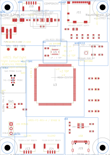
The preferred candidate prioritizes sensor separation and inspectable functional regions over minimum board area. Power conversion occupies the north-west region, the inertial and barometric sensors remain separated from that switching region, communication connectors are arranged around accessible edges, and the microcontroller retains local decoupling support.
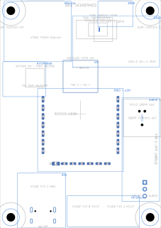
Twenty-one schematic footprints are placed on the bottom side. They are limited to local decoupling, VCAP, VDDA, USB, and related support parts; sensors, external connectors, and other tall or mechanically critical components remain on the top side.
Sensor isolation
The BMI088 center is 14.0 mm from the board mechanical center and 35.725 mm from the nearest mounting hole. Axis marks and an isolation region are present to make orientation and mechanical review explicit.
These distances are placement metrics, not proof of vibration isolation. The airframe coordinate transform, package orientation, local stiffness, fastener loading, modal behavior, and vibration transfer still require human and physical verification.
The BMI088 placement is a review candidate. It is not an approved aircraft sensor transform or a validated vibration-isolation solution.
Power separation
The J1 input, D1 protection, F1 fuse, CIN1 input capacitor, U2 buck regulator, L1 inductor, COUT1 output capacitor, RPG1 resistor, and TP1–TP3 test features are grouped in the north-west power region.
The BMP390 center is 30.0 mm from the regulator and 26.907 mm from the inductor. Those distances document placement separation only. No switch-node copper, input-current loop, ground-return path, thermal-via field, or power-plane implementation exists yet.
Connector and media access
Edge intent is recorded before routing: GNSS exits north, the microSD card and removal envelope exit north, Telemetry A and Telemetry B exit south, and USB-C exits south with its PCB-edge datum aligned at y = 185.000 mm.
The placement view does not prove real cable bend radius, latch access, tool clearance, mating retention, insertion force, enclosure clearance, or serviceability. Physical samples and a calibrated 1:1 print are required before connector access is accepted.
| Interface | Recorded access direction |
|---|---|
| GNSS UART + PPS | North / outward |
| microSD | North / outward extraction |
| Telemetry A | South / outward |
| Telemetry B | South / outward |
| USB-C | South / outward; datum aligned to board edge |
| Tag-Connect SWD | Top-side access |
| Debug UART | South-west access region |
BMP390 pressure-port protection
One 0.9 × 0.9 mm rule area protects the BMP390 pressure-port region from pads, tracks, vias, and copper zones. The digital placement view keeps the port visually unobstructed and marks that it must not be conformally coated.
The rule area does not validate enclosure venting, static-pressure behavior, foam selection, airflow disturbance, contamination protection, moisture resistance, or assembly handling. Those remain mechanical and physical test questions.
Validation results
The Stage 6 placement validation record reports PASS with 16 of 16 checks passed. The frozen Stage 5C electrical record remains at zero ERC errors and zero ERC warnings, while the placement DRC reports zero placement violations.
The checker also confirms that all footprint library identifiers resolve and that 352 schematic pin/net assignments match the board. These are database-consistency results—not measurements from manufactured hardware.
- 0 ERC errors and 0 ERC warnings at the retained schematic baseline.
- 0 placement DRC violations.
- 0 unplaced populated components.
- 0 tracks, 0 vias, and 0 copper zones.
- 16 placement-validation checks passed; 0 failed.
- 352 schematic pin/net assignments match.
What remains unrouted
The ratsnest remains intentionally visible. There are 54 multi-node nets and 218 unrouted connectivity items. These are expected for an unrouted board and were not excluded, suppressed, or relabeled as resolved.
No controlled-impedance pair, USB route, SDMMC bus, sensor bus, clock path, power loop, ground return, via strategy, copper zone, or final layer transition has been implemented. Stage 7 routing has not started.
A complete placement is not a completed PCB. The full connectivity burden remains visible for the next controlled gate.
Human mechanical checks before routing
Routing remains blocked until a human reviewer prints the supplied PDF at 100% scale, verifies the calibration feature, places physical samples or manufacturer-scaled references over the footprints, and records the result.
- Confirm the 60 × 85 mm outline, four M3 holes, edge offsets, screw-head envelopes, and fastening access.
- Verify physical samples and pin-one orientation for the USB-C connector, microSD socket, power connector, GNSS, telemetry, debug, and Tag-Connect interfaces.
- Check mating-part fit, insertion and removal direction, cable bend radius, latch access, tool clearance, and enclosure-wall clearance.
- Confirm BMI088 package orientation, axis convention, keep-out intent, and relationship to mounting stiffness.
- Confirm BMP390 pressure-port location, vent path, foam or membrane strategy, airflow exposure, contamination protection, and no-coating instruction.
- Review component height, bottom-side clearance, assembly access, and the preliminary enclosure volume.
- Record every discrepancy before any route or manufacturing output is created.
Missing 3D models
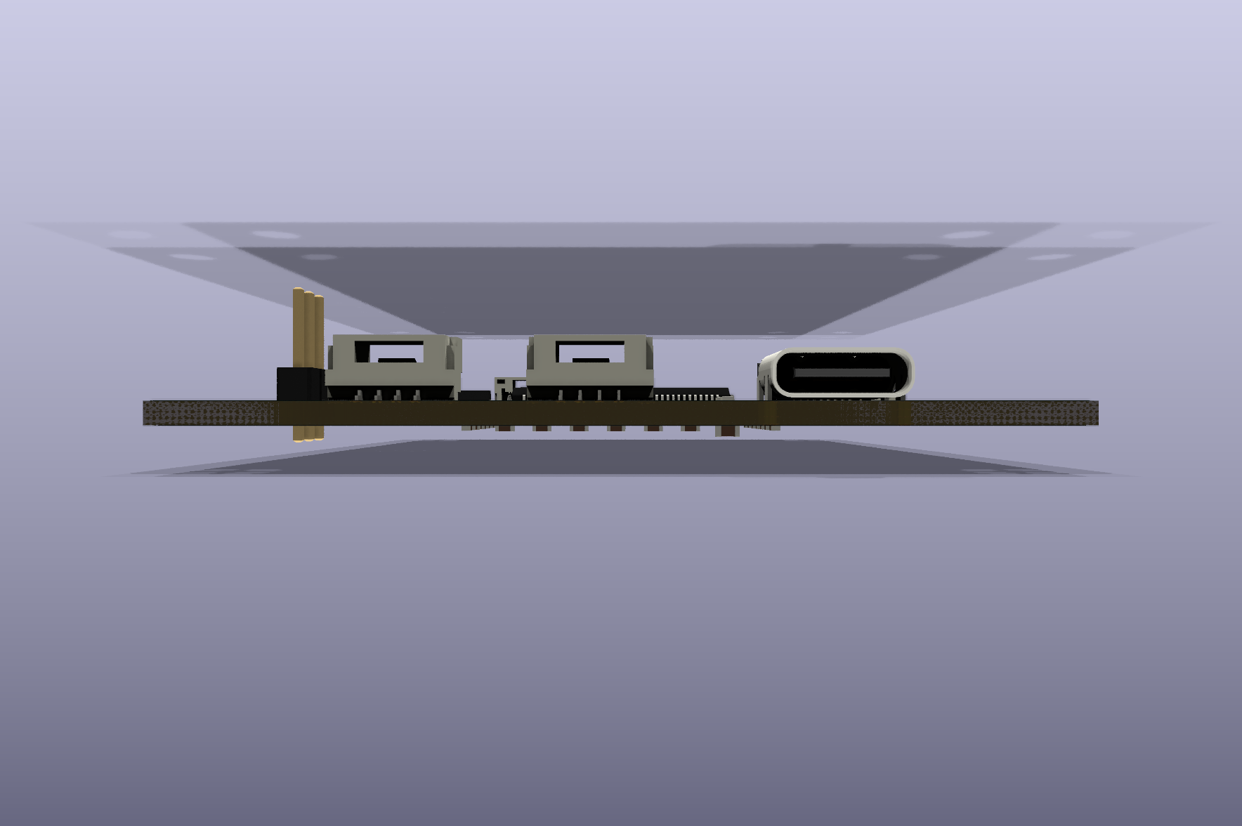
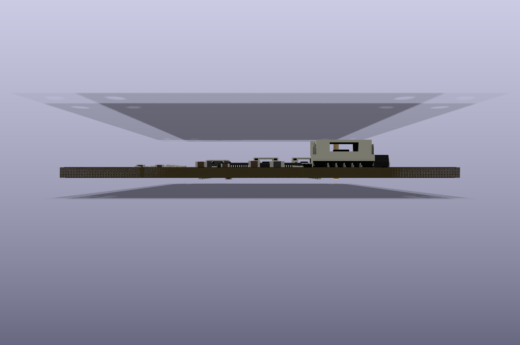
The KiCad 3D review has unresolved or missing body models for J1, J4, J11, U2, U7, and TP1–TP3. The available views therefore cannot prove full connector height, body envelope, insertion clearance, heatsink or inductor envelope, or test-point access.
A missing 3D model is not the same as a footprint or pad failure. The associated footprints resolve and passed the documented database checks, but mechanical proof remains incomplete until accurate models or physical measurements are reviewed.
The Stage 7 routing gate
Stage 7 is planned as controlled routing work after mechanical sign-off. It has not started. The gate must first resolve the 1:1 footprint review, connector access, mounting geometry, sensor orientation, pressure-port strategy, missing 3D bodies, enclosure assumptions, and any placement corrections.
Only then can routing examine high-current loop geometry, USB and SDMMC signal paths, sensor buses, timing signals, reference planes, return-current continuity, power distribution, thermal separation, test access, and manufacturability constraints.
Current gate: HUMAN MECHANICAL REVIEW. Next planned gate: CONTROLLED PCB ROUTING.
Evidence and downloadable review material
The gallery below reproduces the generated top, bottom, front-edge, and rear-edge KiCad review views without adding a promotional composite. The downloadable PDF is the 1:1 placement-review artifact intended for calibrated printing and physical inspection.
The 3D images are KiCad renders, not photographs of a manufactured board. Several models are missing, so the renders must not be used as final mechanical proof.
Technical review and correction path
The milestone is published before routing so connector, footprint, mechanical, sourcing, sensor-placement, pressure-port, power-layout, and manufacturability concerns can be raised while change remains inexpensive.
Corrections will be recorded through the public corrections process. A future revision may alter placement, outline, connector choice, or mechanical assumptions without erasing this Stage 6 evidence boundary.
We welcome technical review, sourcing suggestions, footprint checks, and manufacturability feedback before placement is accepted and routing begins.
Placement evidence gallery
These are direct KiCad outputs. They document the digital placement state and do not represent manufactured or physically validated hardware.
Challenge the assumptions.
We welcome technical review, sourcing suggestions and manufacturability feedback before placement and routing begin.